



Many material properties depend on how electrons are arranged inside a material. Their distribution determines, for example, whether a material conducts electricity or displays magnetic behaviour. Understanding how electrons organise themselves at the atomic scale is therefore one of the major challenges in materials science. Now, a team led by researchers at the Institute of Materials Science of Barcelona (ICMAB-CSIC) has developed a new technique that, for the first time, reveals how electrons are organised inside materials with an unprecedented level of detail.
Until now, available techniques could only provide an overall picture of electronic structure. They could not reveal in detail how electrons vary from one atom to another, either at the surface or deeper within the material. “This type of instrument is like opening a box that until now has been closed,” says Jaume Gàzquez, ICMAB-CSIC researcher and one of the corresponding authors of the paper published in Nature Materials. “We can now observe phenomena that simply could not be seen before.”
The work was carried out in collaboration with the University of Chinese Academy of Sciences, Uppsala University (Sweden), the University of Washington (United States), and the Pacific Northwest National Laboratory (United States). The project brought together expertise in advanced microscopy, theoretical simulations and materials synthesis.
A versatile tool that opens up a new area of research
Electrons do much more than determine whether a material conducts electricity or exhibits magnetic properties. The way they are arranged around atoms also influences many other physical and chemical characteristics. In some materials, even a slight change in structure can rearrange the distribution of electrons and alter the material's behaviour. Scientists have studied these effects for decades, but progress has been limited by the lack of sufficiently detailed information.
The researchers emphasise that the methodology is broadly applicable and could be used in many other areas of materials research. To demonstrate the technique, they investigated a manganese oxide material, chosen because of its interesting electrical and magnetic properties. They found that slightly compressing the material changes the way electrons are arranged inside the atoms, while stretching it produces a different electronic response. These differences are invisible to conventional techniques, yet they can directly influence properties such as conductivity and magnetism.
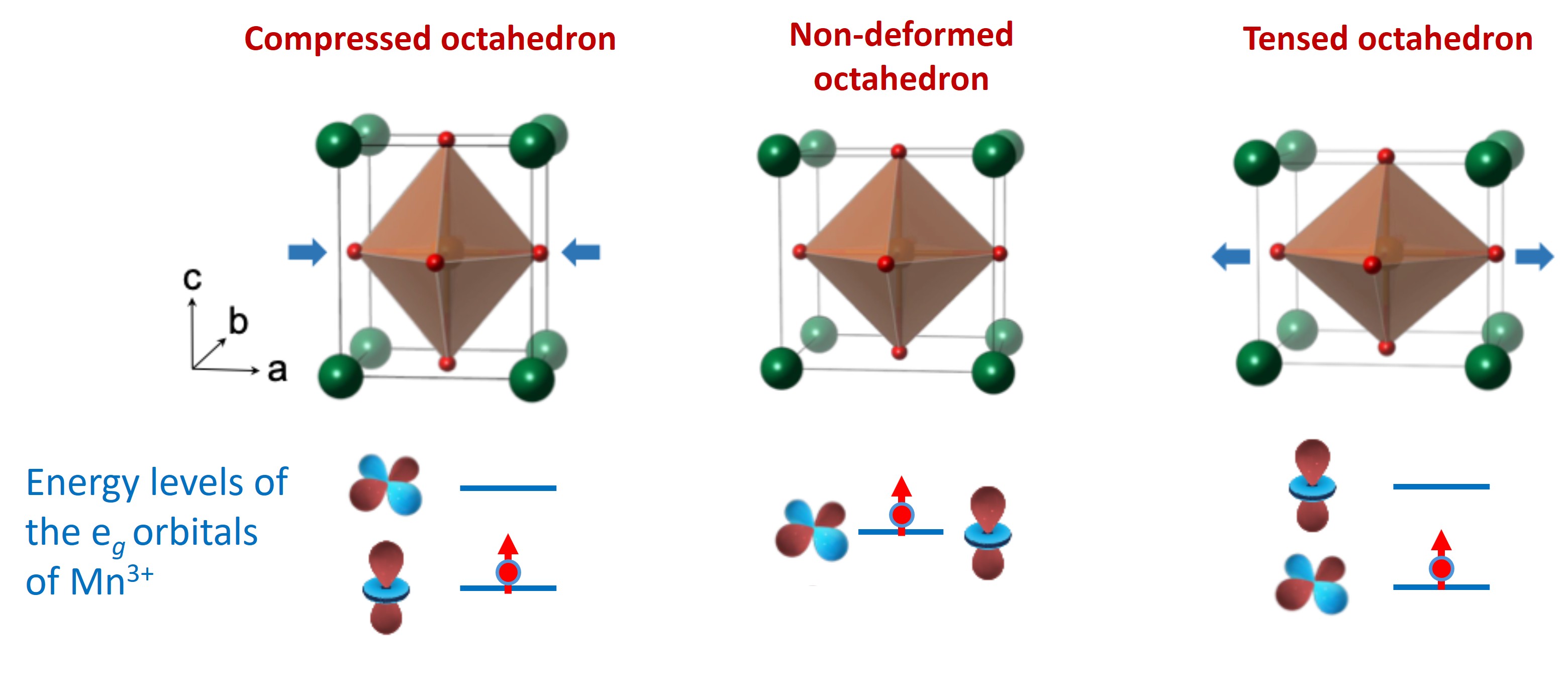
The new approach allows these changes to be detected locally and tracked within the same material with unprecedented precision. Because it can be implemented using advanced electron microscopes that already exist today, it could become a powerful tool for studying complex structures in which electronic properties vary over extremely small distances.
For Jaume Gàzquez, “the main novelty is that we can now study what happens in very specific regions of a material, down to the level of individual atoms.” According to the researcher, this capability will be particularly useful for investigating defects or interfaces between different materials, areas where unusual properties often emerge that are absent from the rest of the material.
How the new technique works
The method is based on an advanced form of electron microscopy. Researchers direct an extremely fine electron beam onto a material and analyse how it interacts with the electrons already present in the atoms. This information can then be used to reconstruct how electrons are distributed and organised at different locations within the material. “It is like illuminating an object from different angles and measuring subtle changes in its response in order to determine how electrons are arranged inside it,” explains Jaume Gàzquez.
Unlike in the popular image of electrons orbiting around an atomic nucleus like planets around the Sun, in reality electrons occupy diffuse regions of space, often described as clouds, which scientists call orbitals. The new technique makes it possible to observe directly how these orbitals are occupied. In other words: the regions where electrons are most likely to be found.
Earlier techniques based on X-rays could not achieve the same level of precision. Rather than taking a “broad snapshot” of a material, the new atomic-resolution approach “scans” every detail of it, producing a much more detailed picture of its electronic structure and revealing variations that previously went unnoticed.
Reference article
Detecting linear dichroism with atomic resolution
Guzman, R., Rusz, J., Li, A., Idrobo, J. C., Zhou, W., & Gazquez, J.
Nature Materials, 2026
DOI: 10.1038/s41563-026-02606-6
> Read the press release in CAT, ENG, ESP
Related posts