

The electron microscopy service was created in 2008 and is mainly dedicated to research groups of the Institute, but it can be accessible to external users as well.
The service consists of a scanning electron microscope (SEM) QUANTA FEI 200 FEG-ESEM installed in September 2008 (substituting an old PHILIPS 515 acquired in 2004 as a result of a process of reallocation between the CSIC centres CID and ICMAB) and a transmission electron microscope JEOL 1210 acquired in 1991. With the acquisition of the new SEM, the service provides ICMAB with a powerful and versatile tool capable to combine routine daily work with cutting-edge research. As a general strategy, this way the service aims at satisfying in-house the increasing demand of high-profile nanostructural characterization, thus eliminating technical limits imposed by external scientific-technical services.
To promote an efficient exploitation, the service offers: 1) Technical support given by two high-profiled (doctor) staff members. 2) Electronic management. 3) Effective user-training system by technical staff, oriented to achieve a maximum degree of self-service.
Technicians


Scientists in charge

User's Committee


Equipment SEM

The Quanta 200 ESEM FEG from FEI is a special and advanced type of high performance scanning electron microscope (SEM). The FEI Quanta 200 FEG is a state of the art field emission microscope that allows nanometer level inspection of materials.
It is equipped with a field emission gun (FEG) for optimal spatial resolution. The instrument can be used in high vacuum mode (HV), low-vacuum mode (LV) (water vapour injection), and environmental SEM mode (ESEM). This makes it possible to study samples in pressures up to 5 Torr. It is engineered to provide maximum data with non-destructive analytical techniques- imaging and microanalysis – from all types of specimens, with or without preparation. The microscope is equipped with an Energy Dispersive X-ray (EDX) system for chemical analysis. Qualitative and quantitative analysis, elemental mapping and linescans can be performed. Lithography and nano-lithography can be performed by a RAITH e-beam.

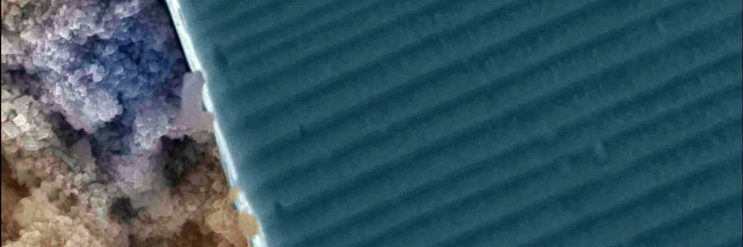
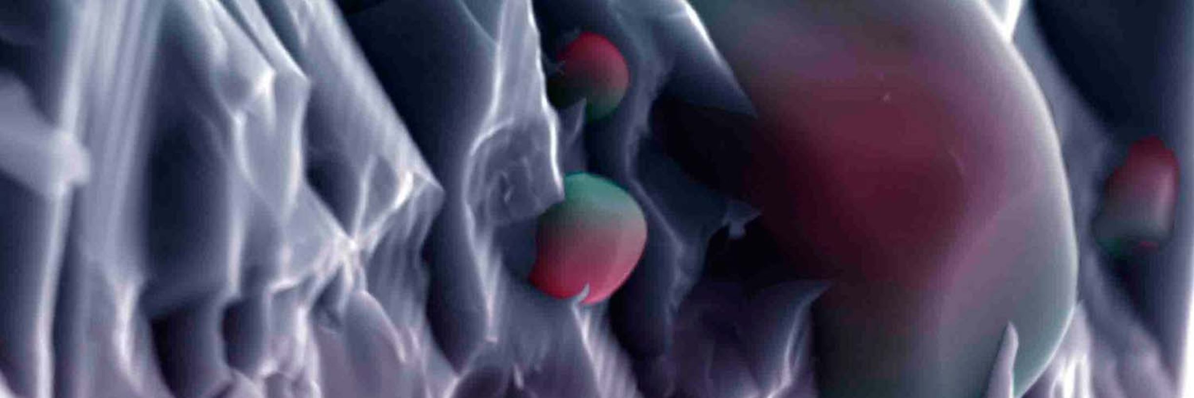
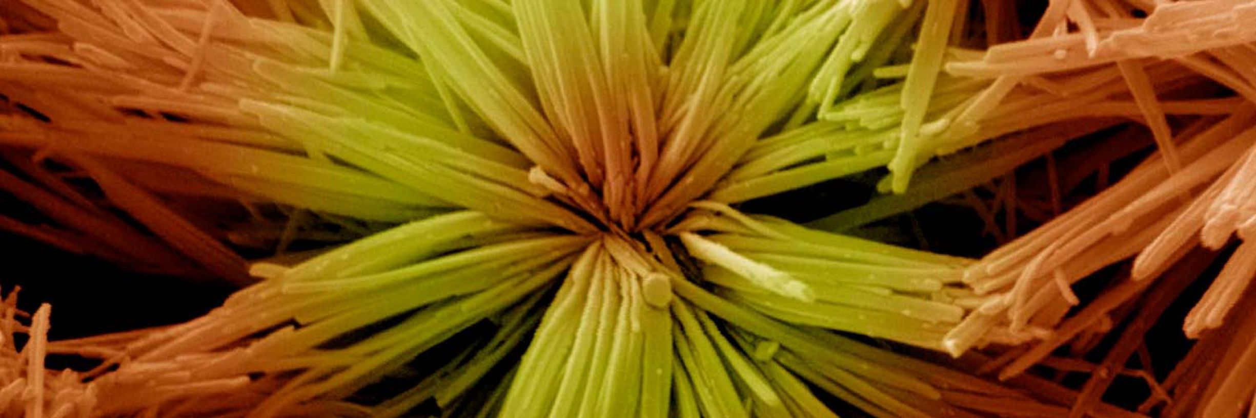
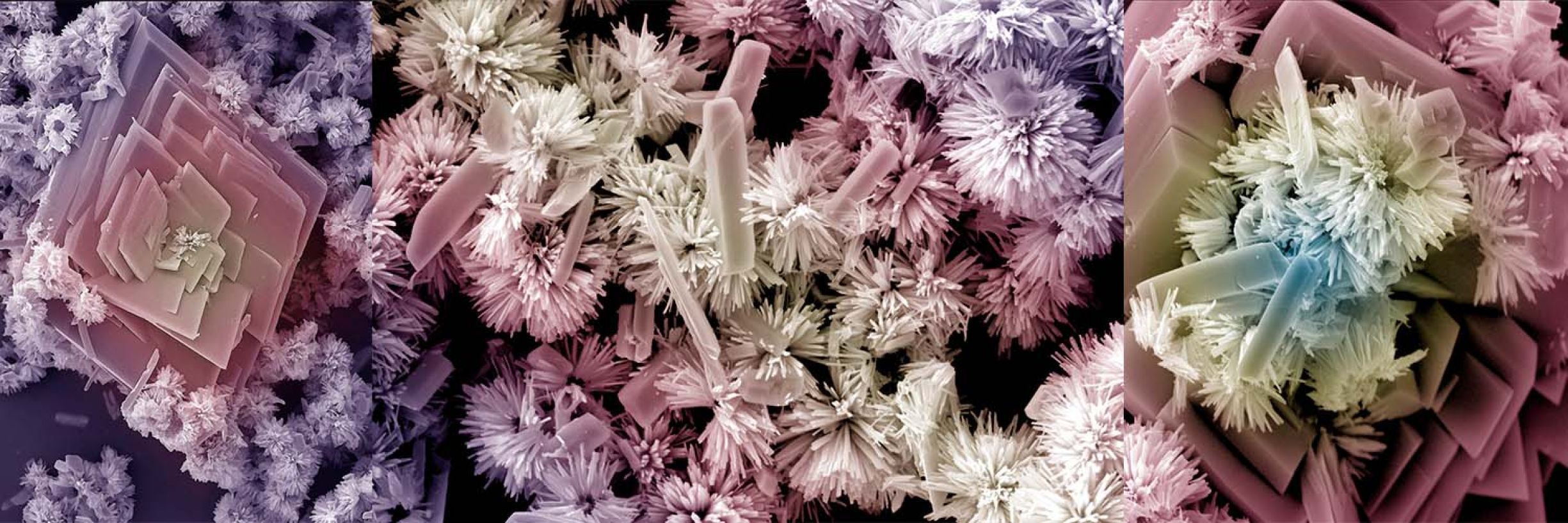
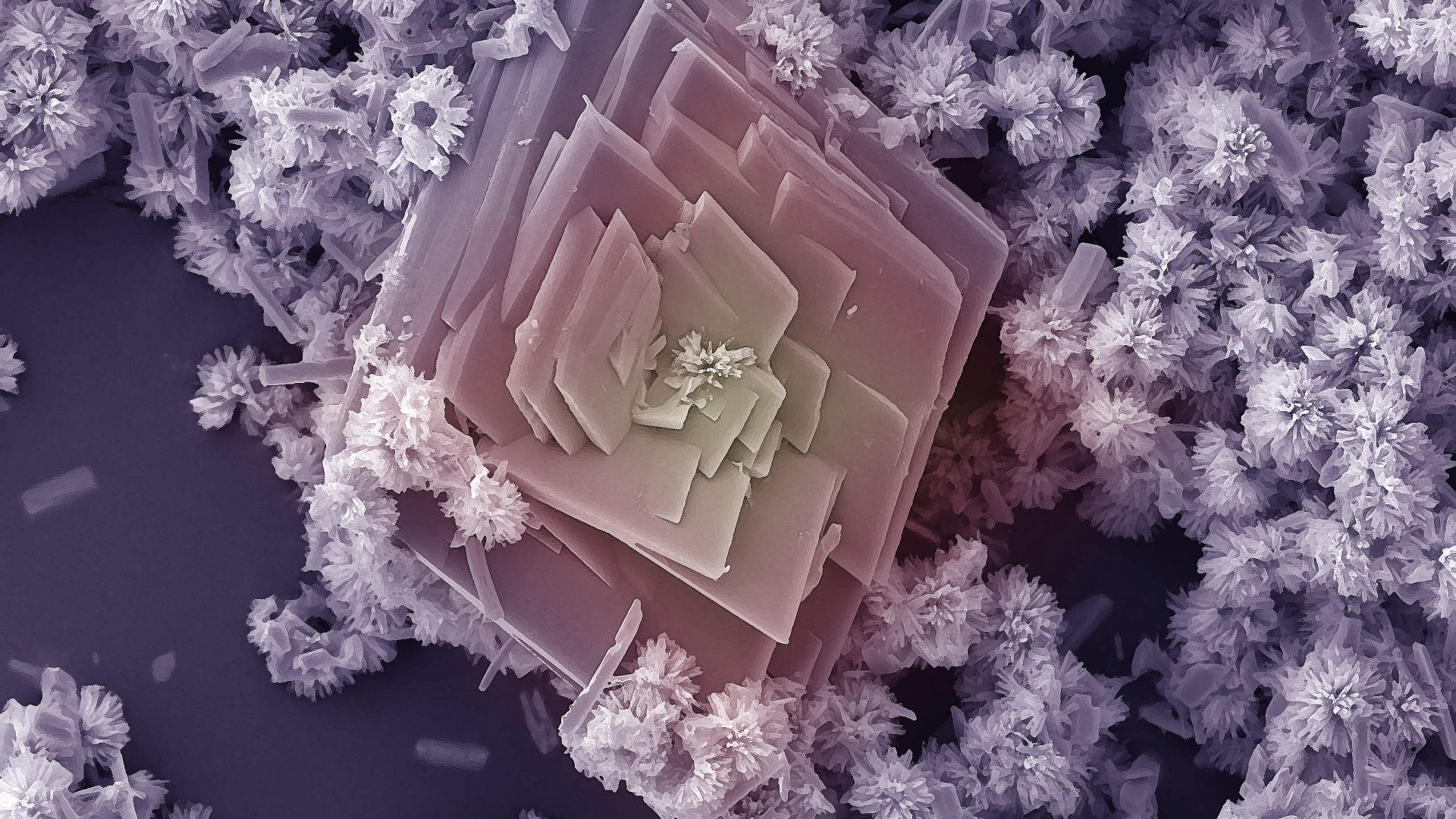
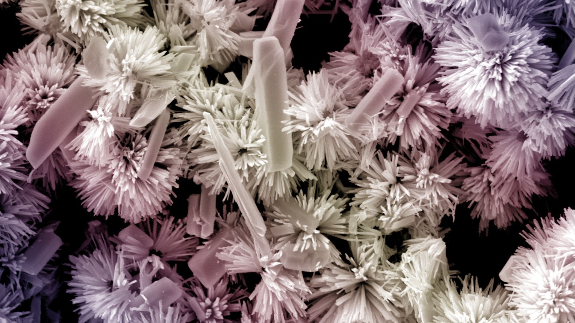
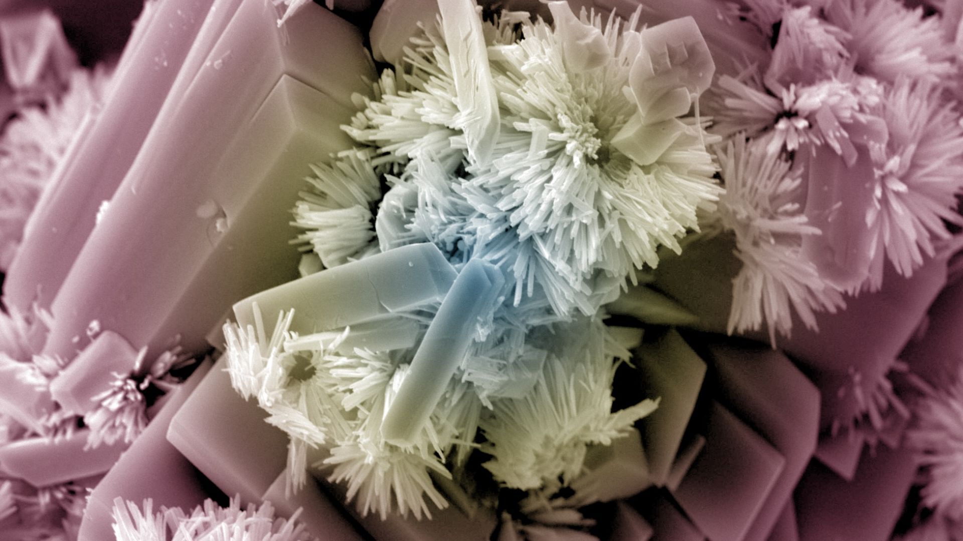
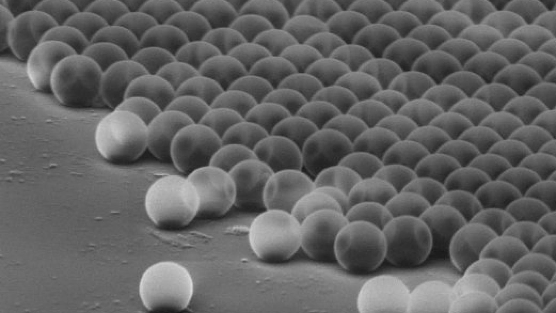
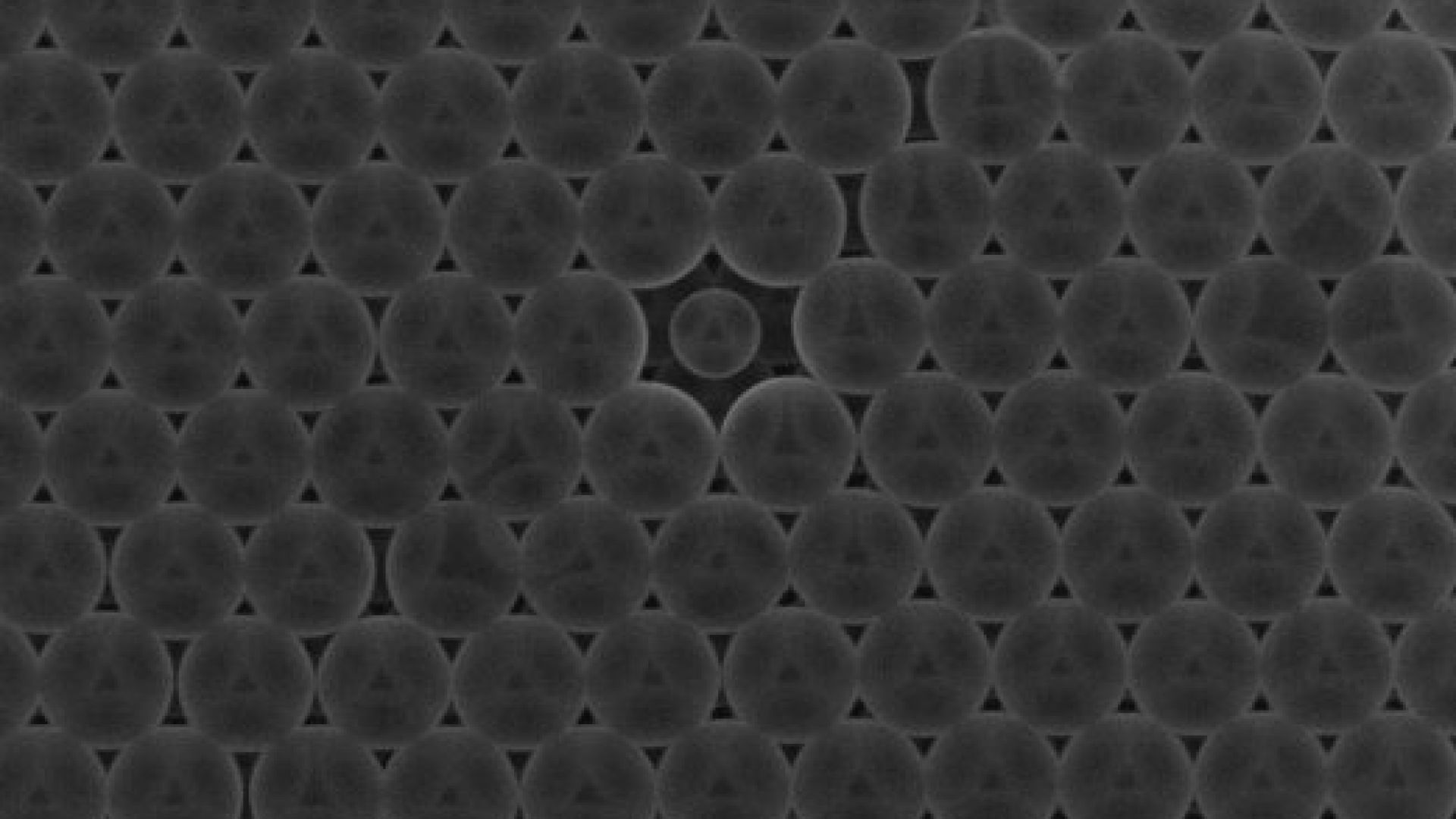
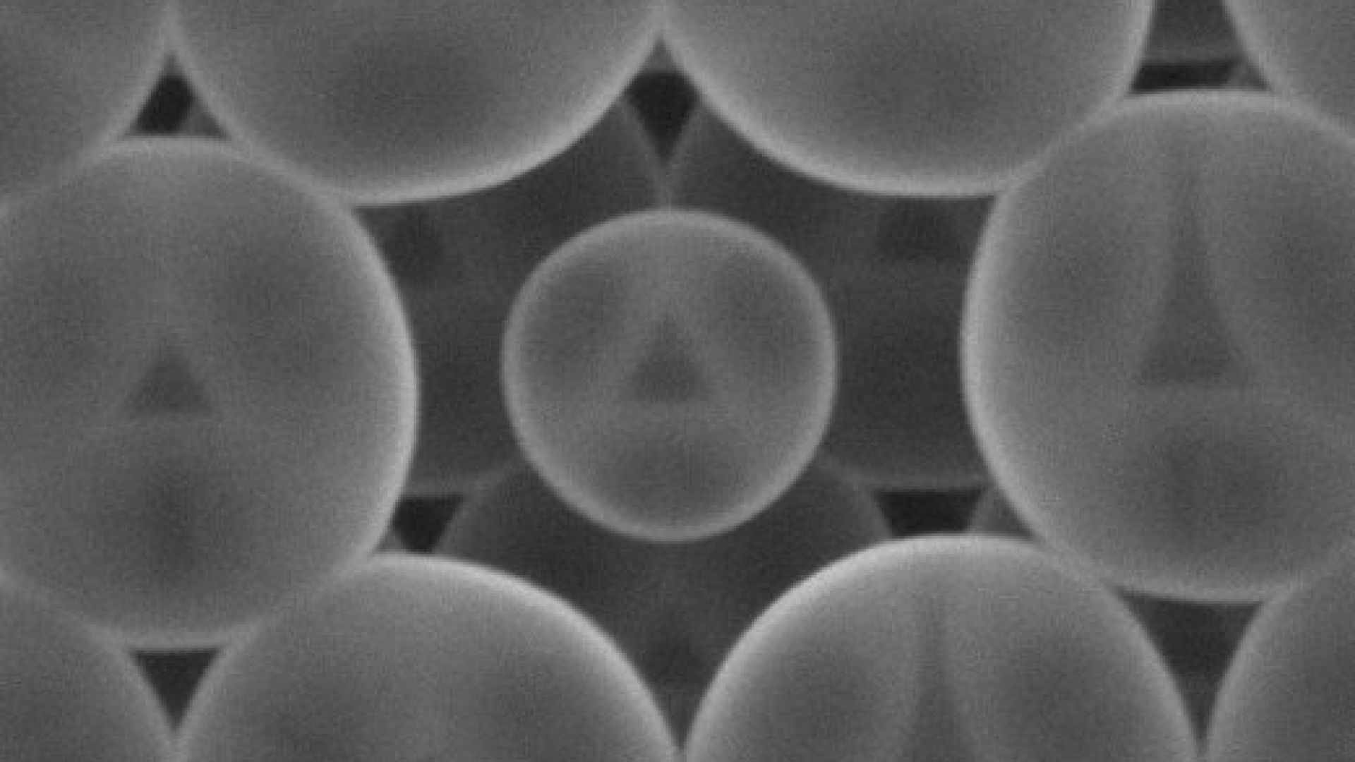
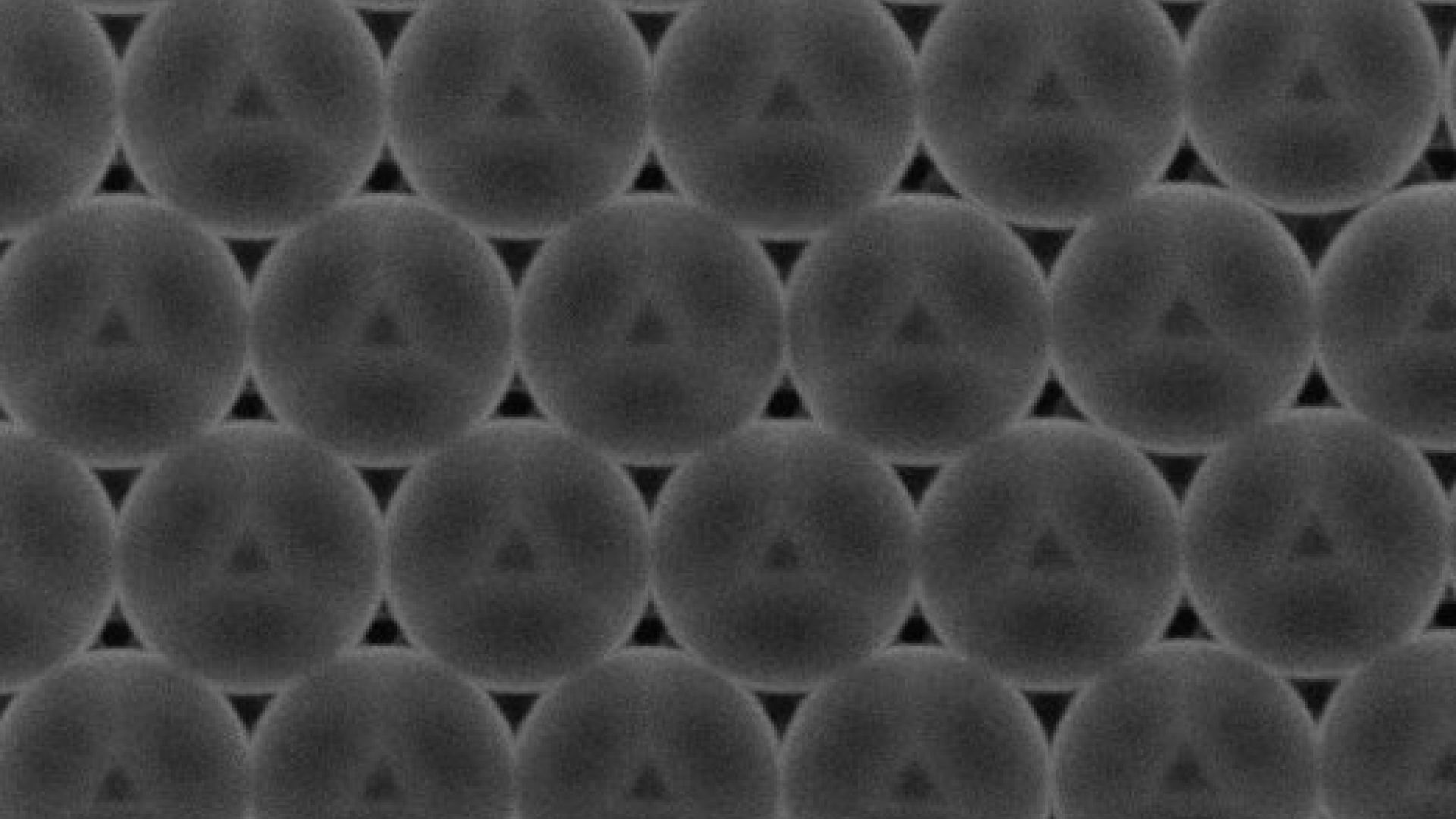
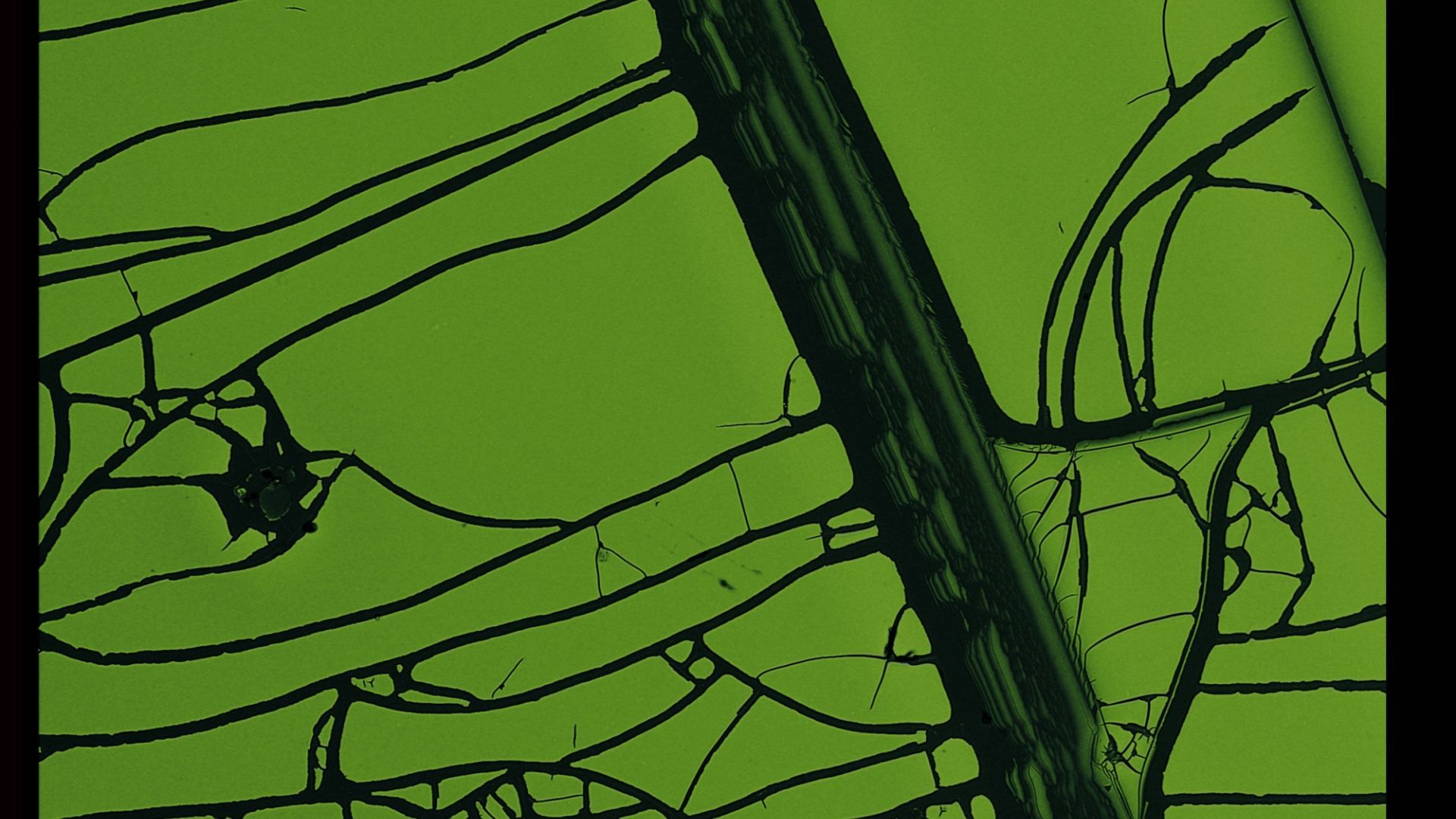
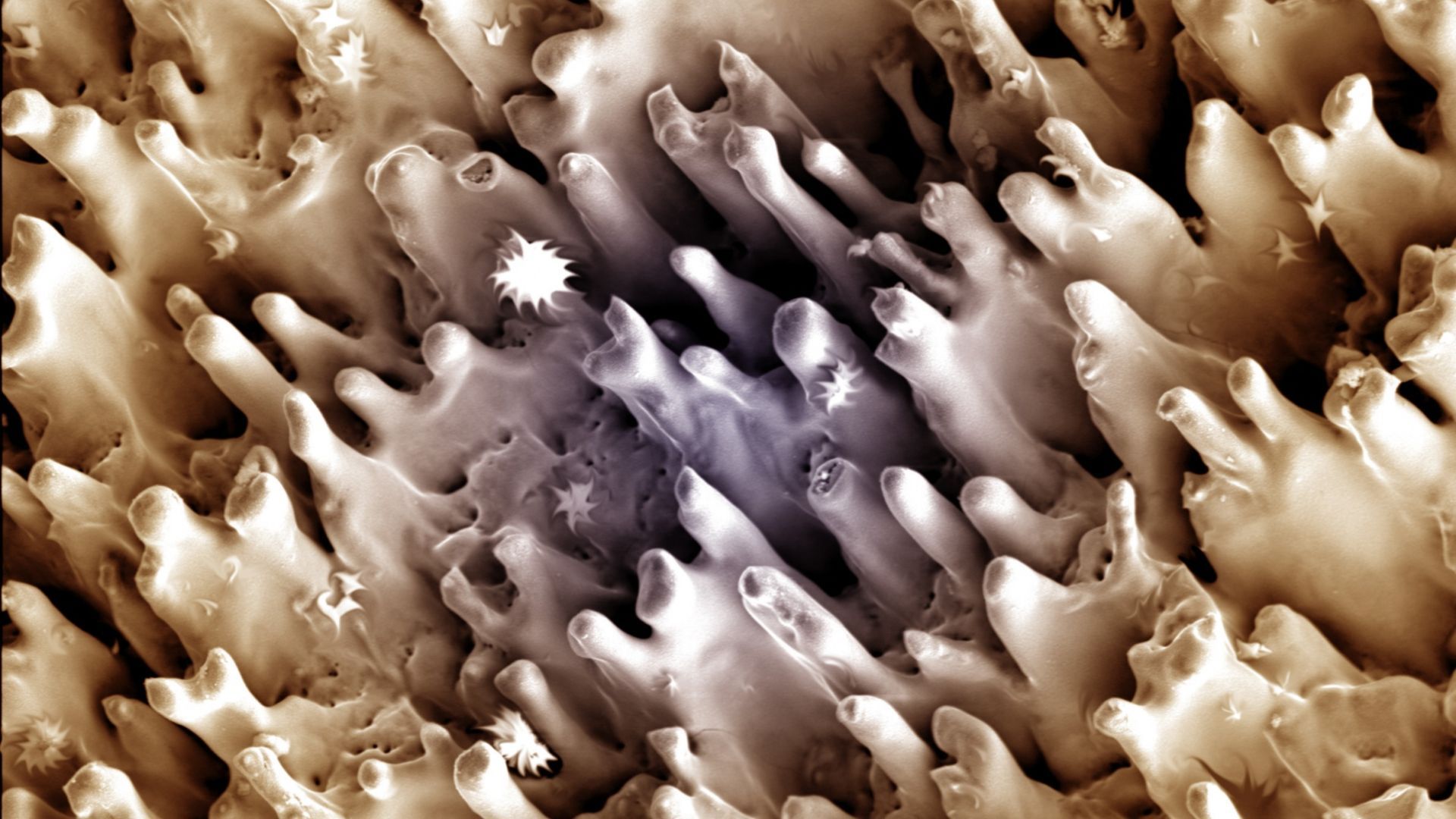
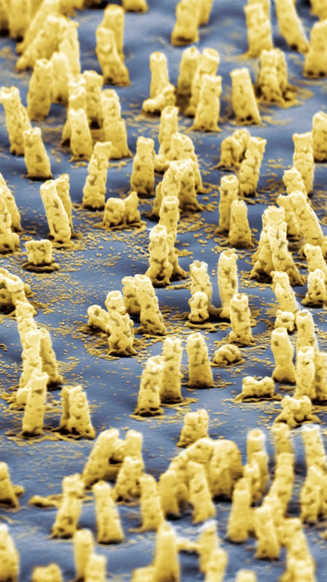
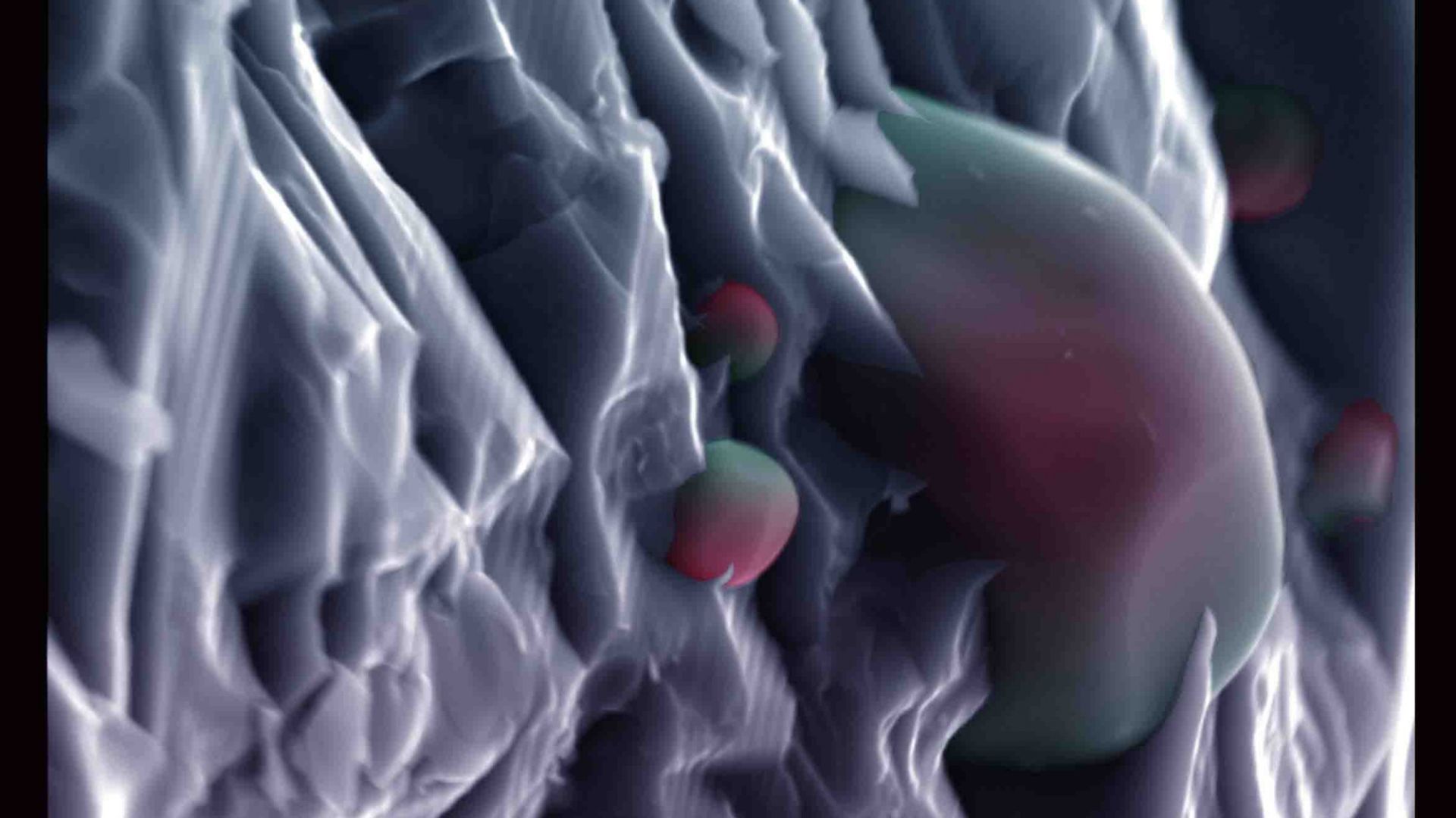
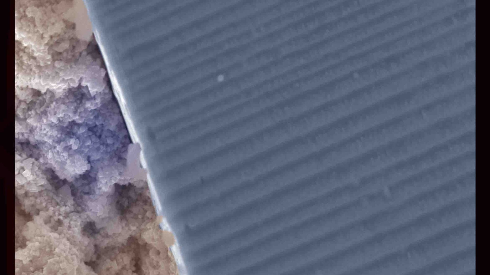
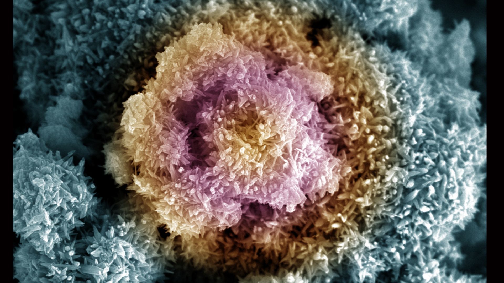
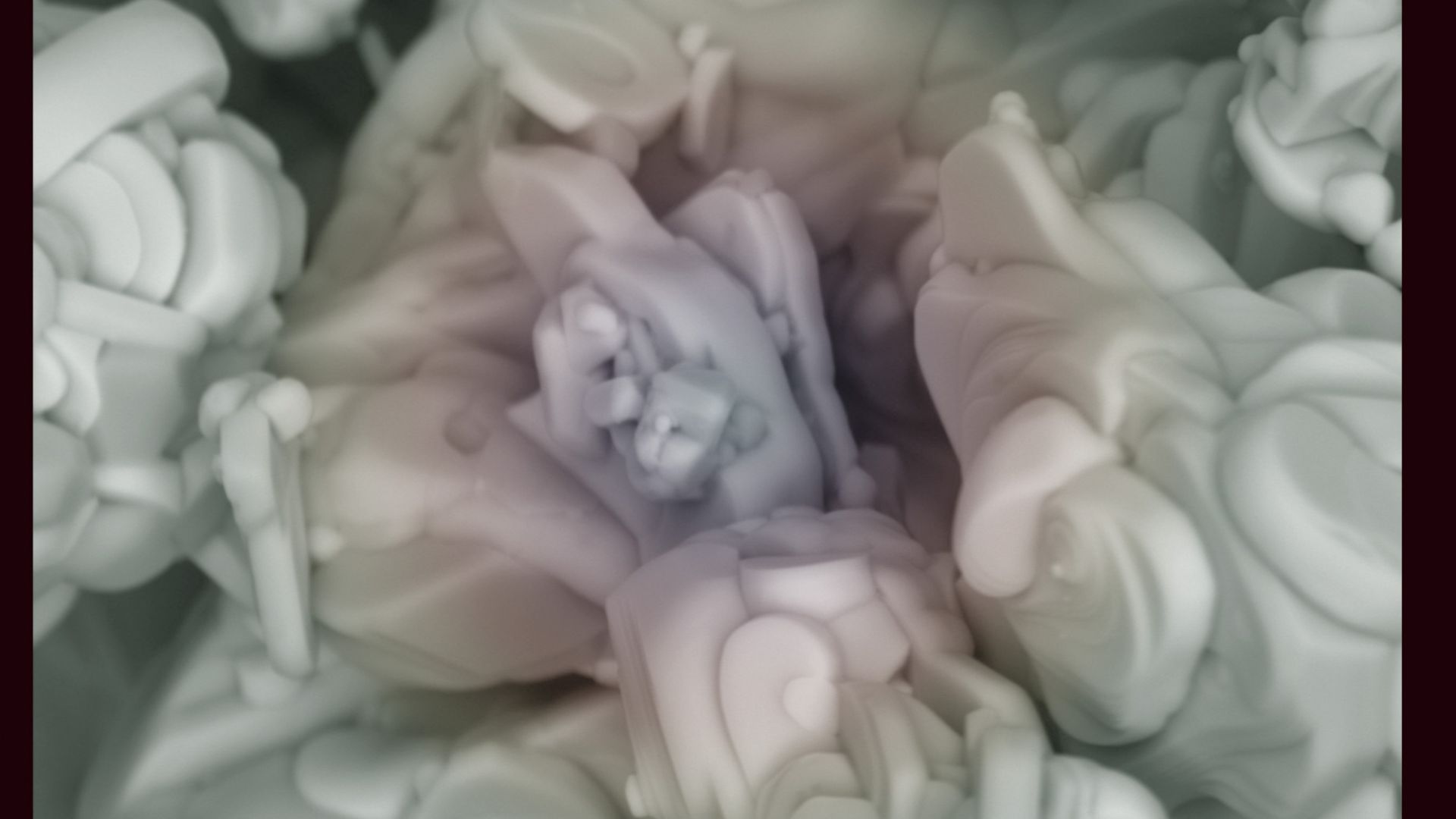
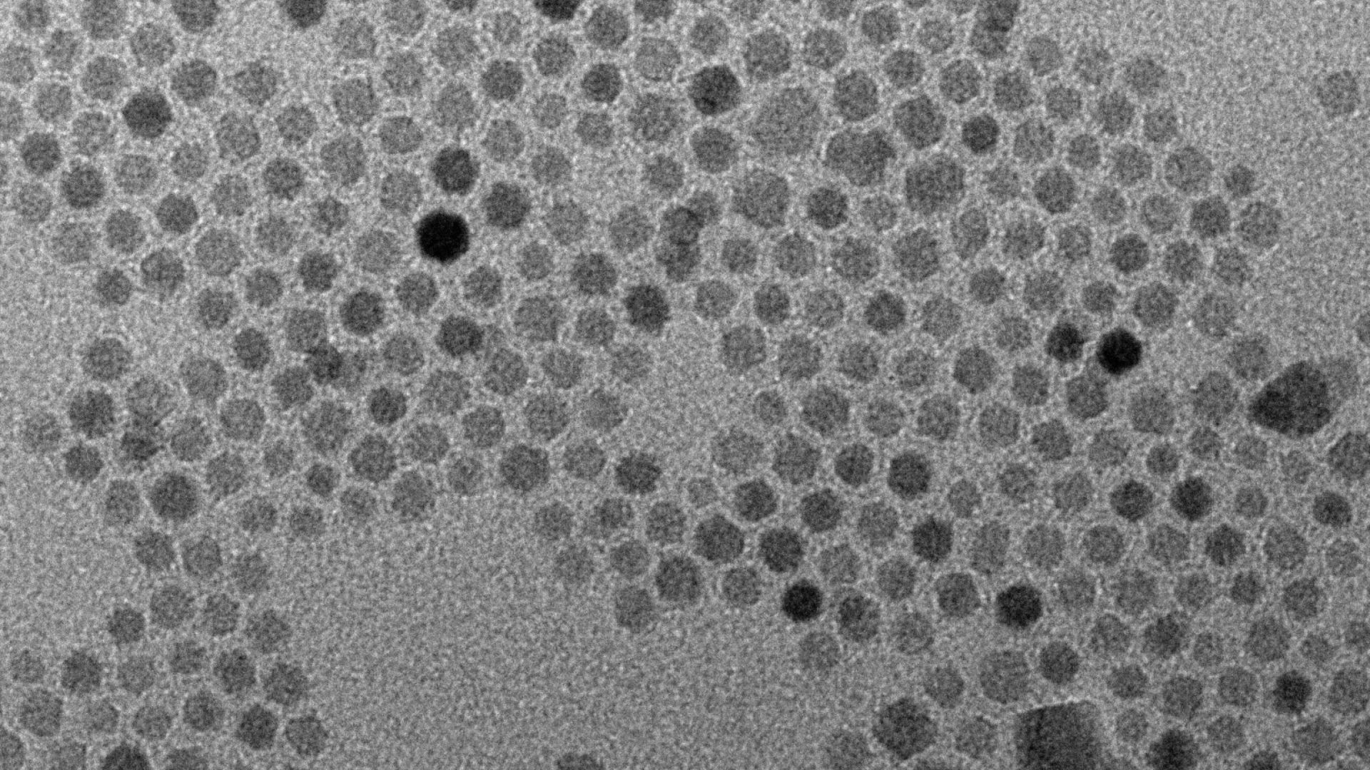
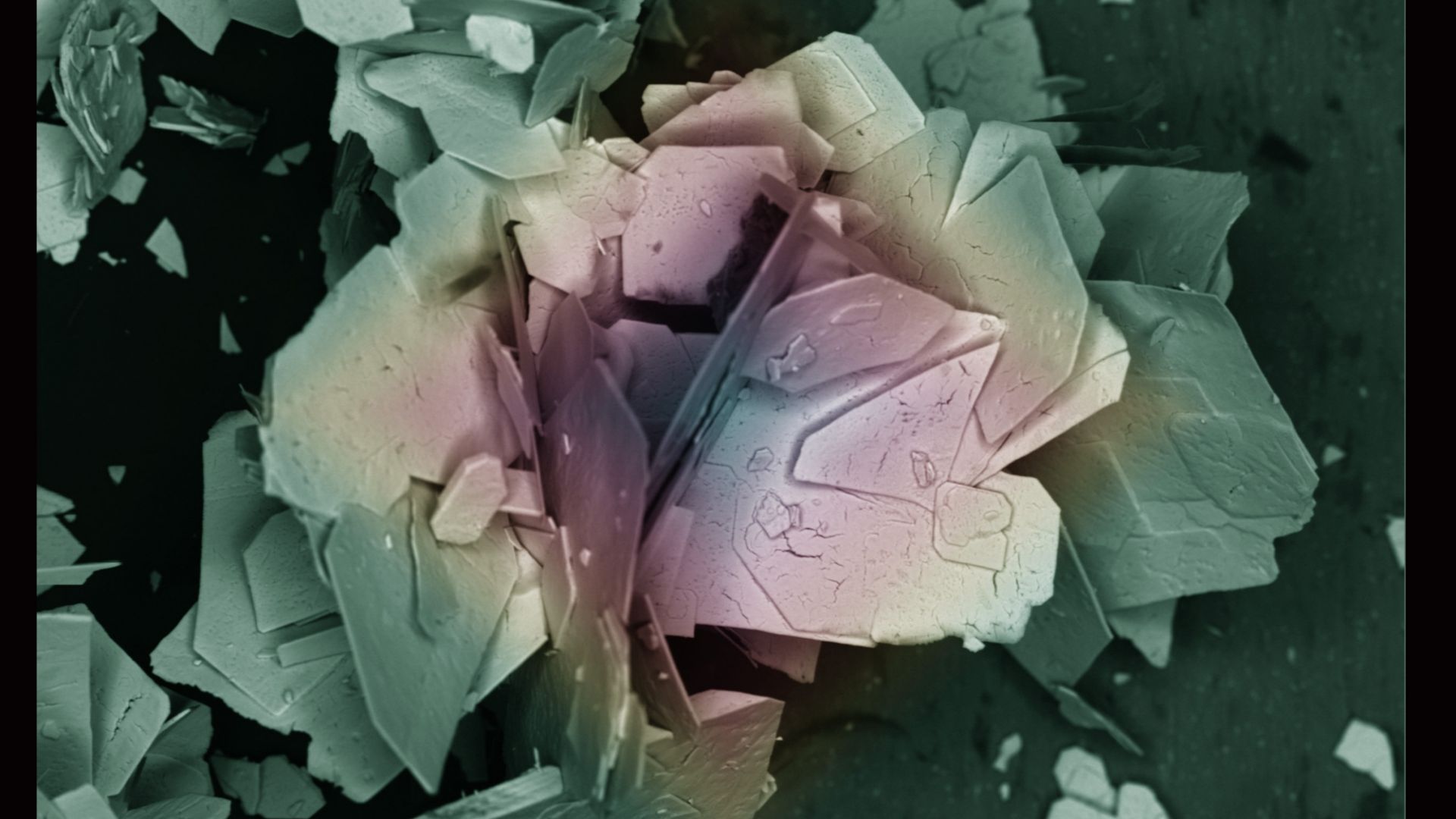
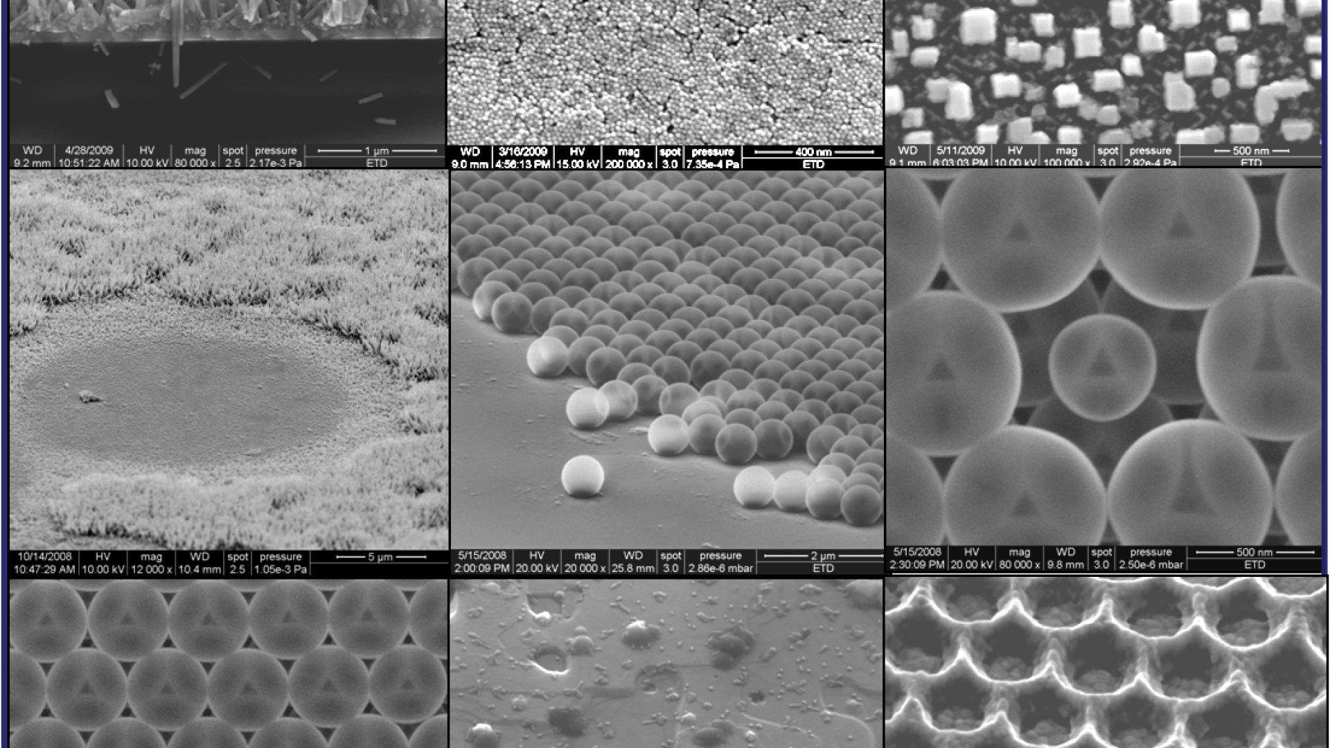
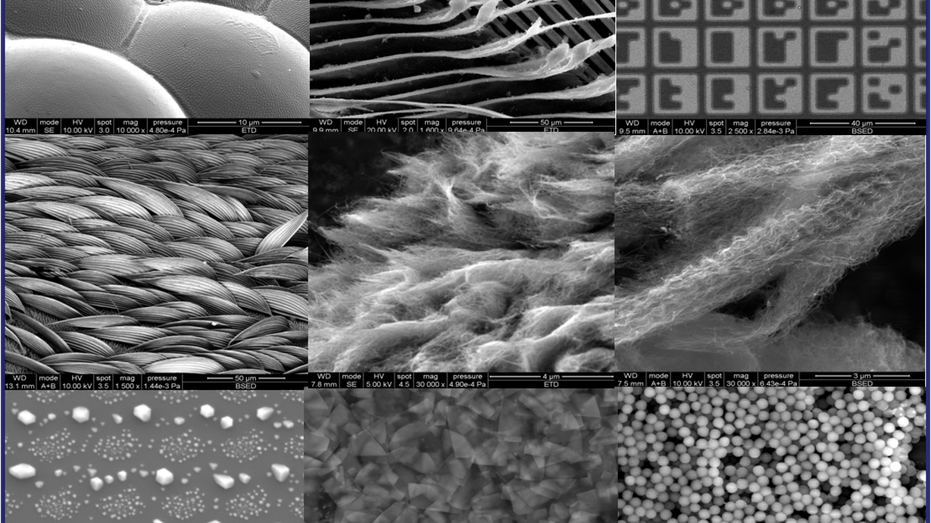
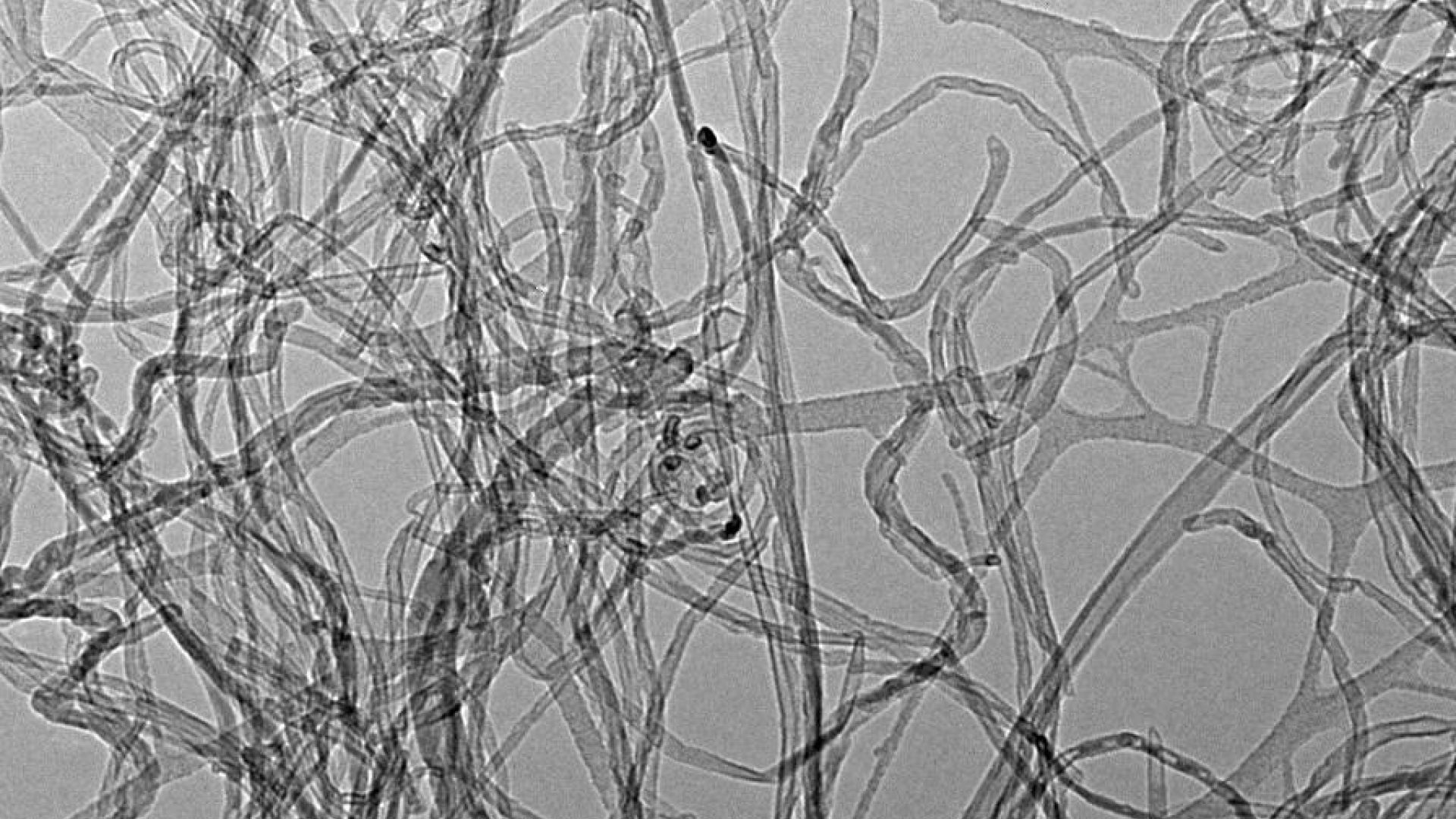
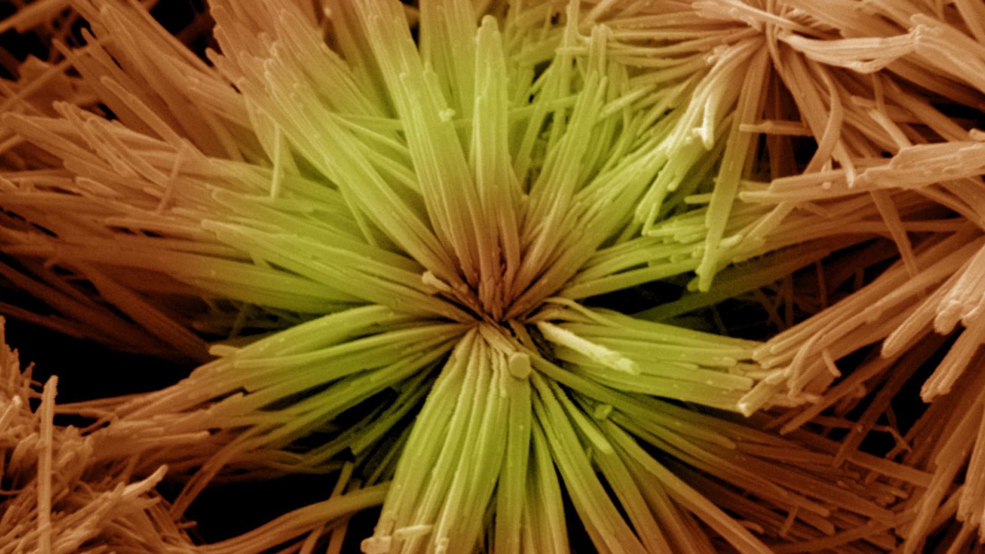
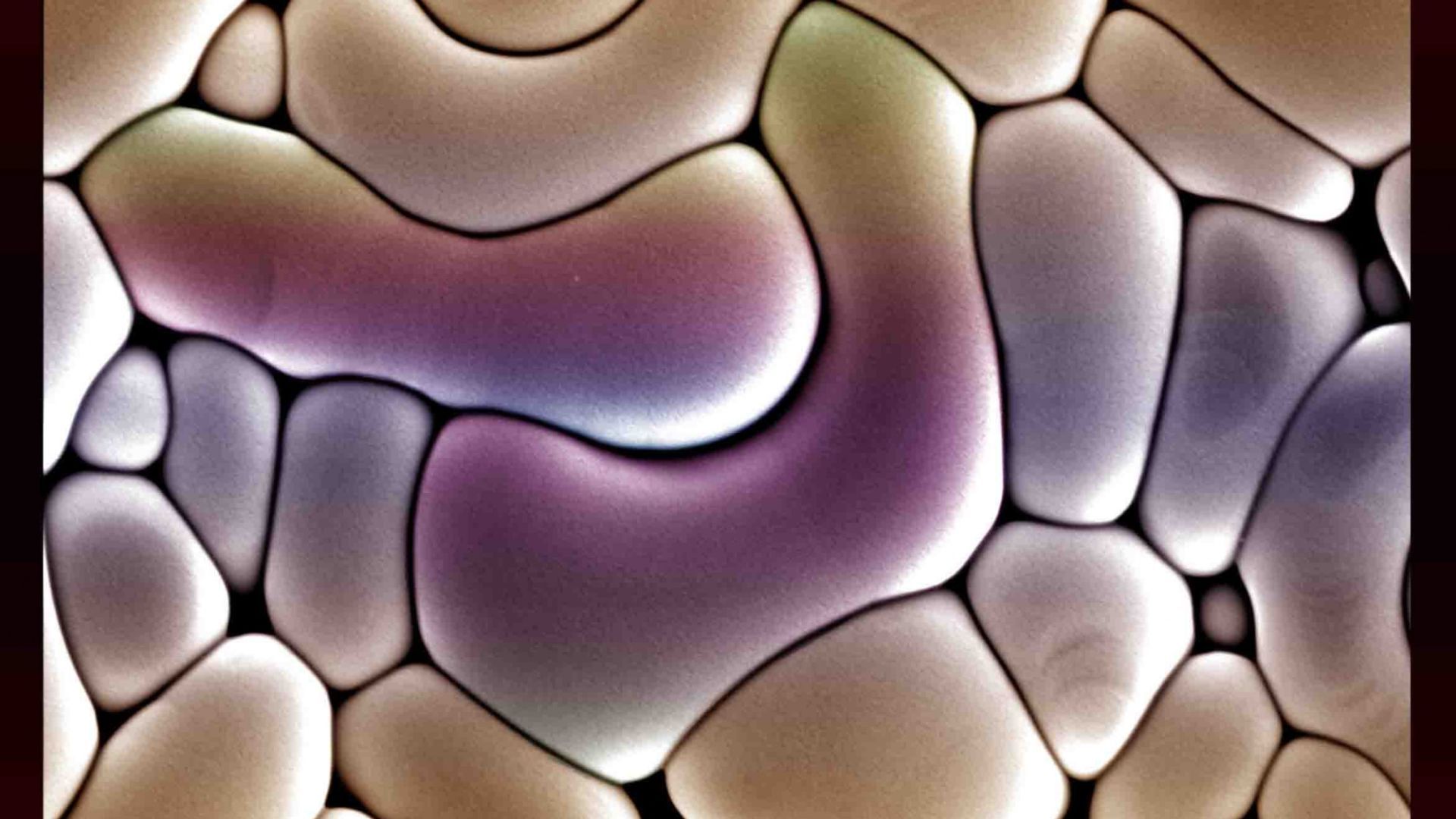
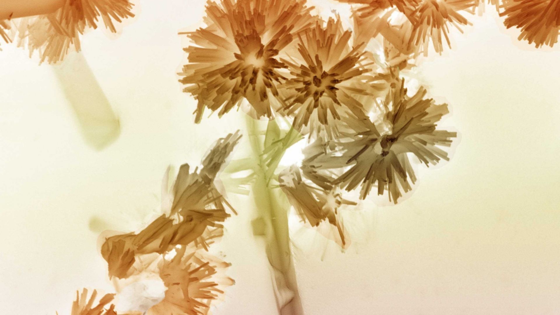
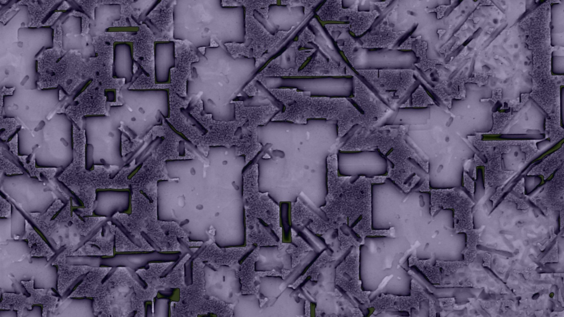
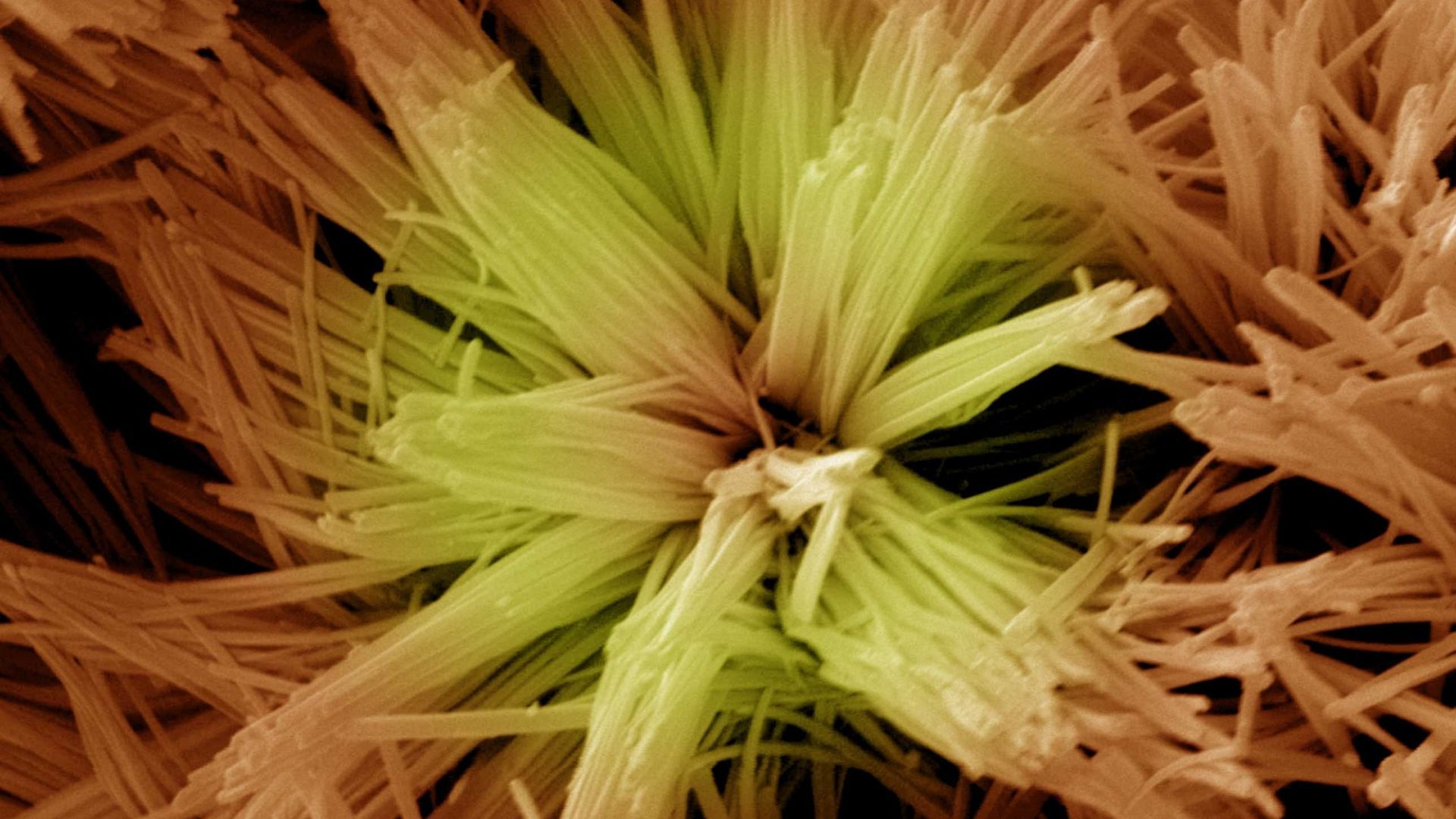
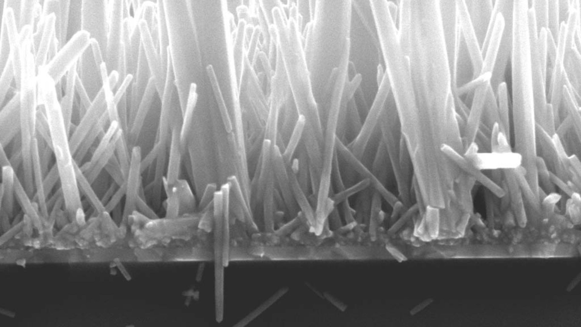
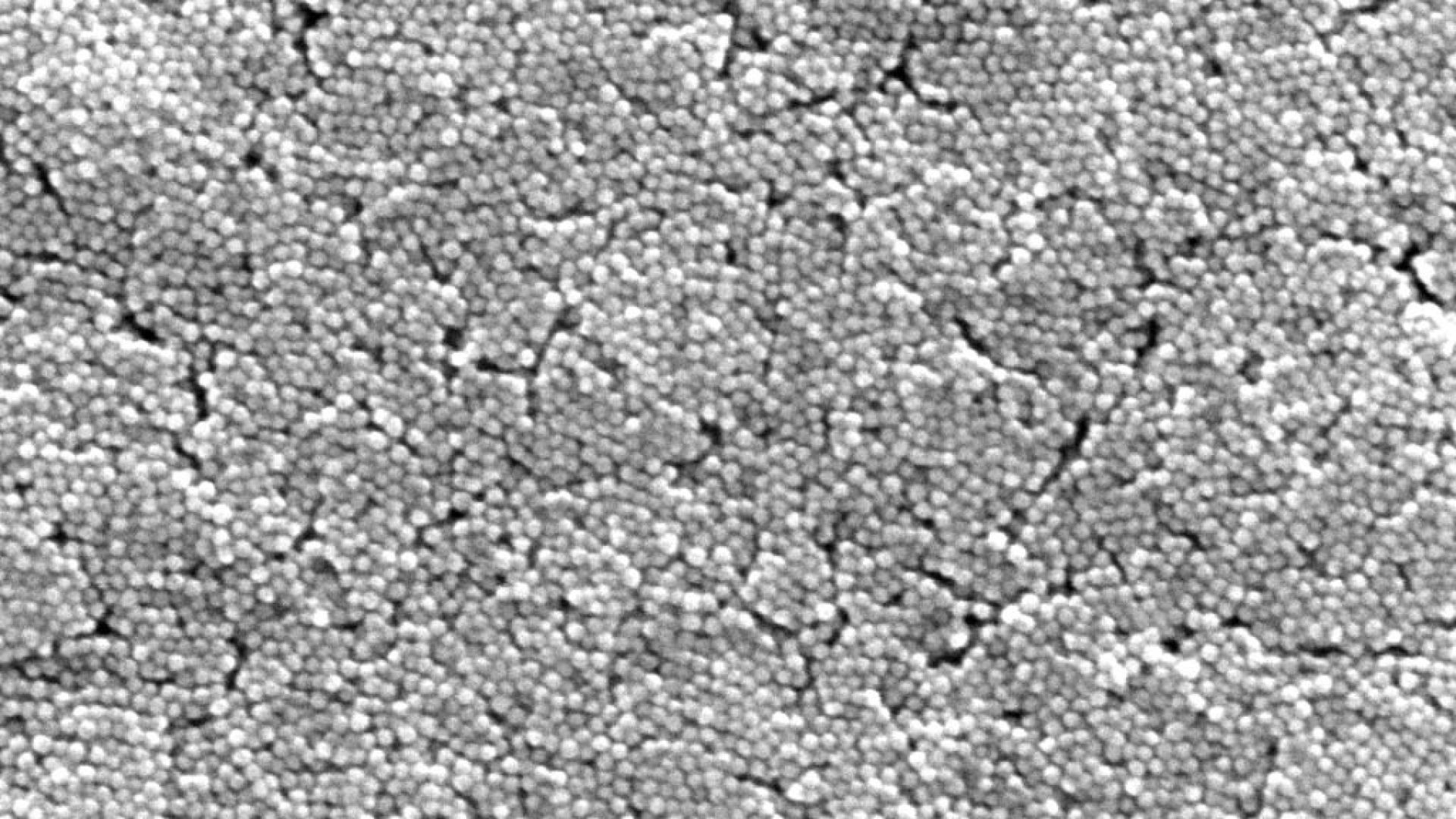
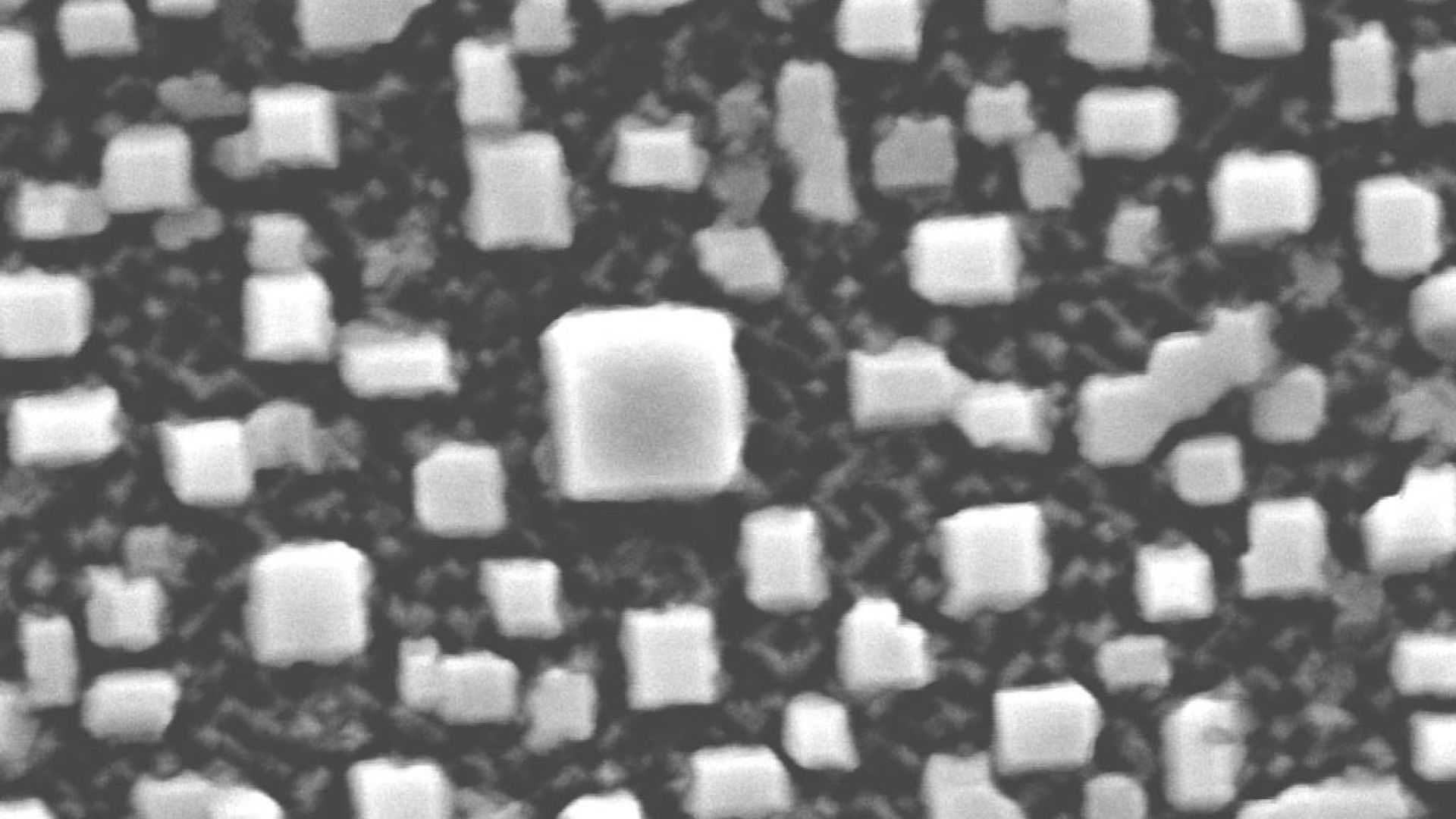
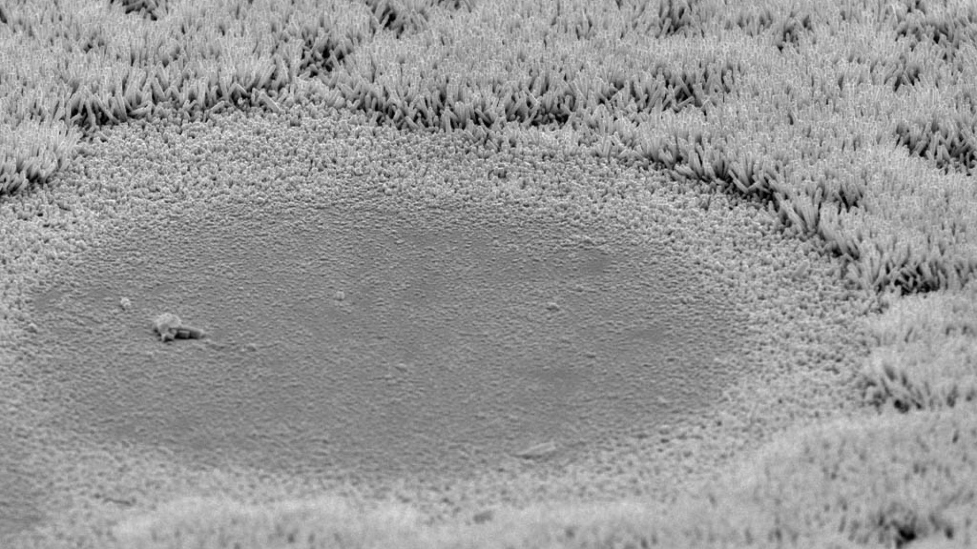
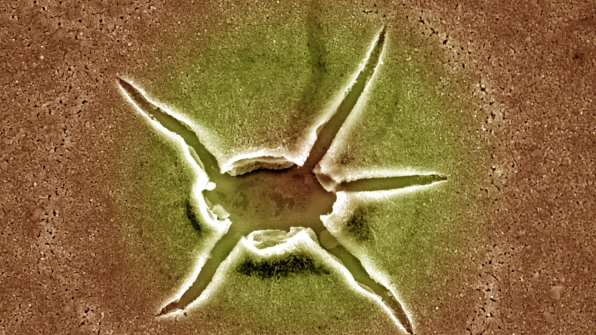
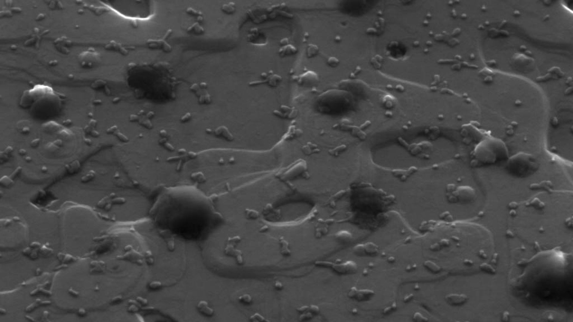
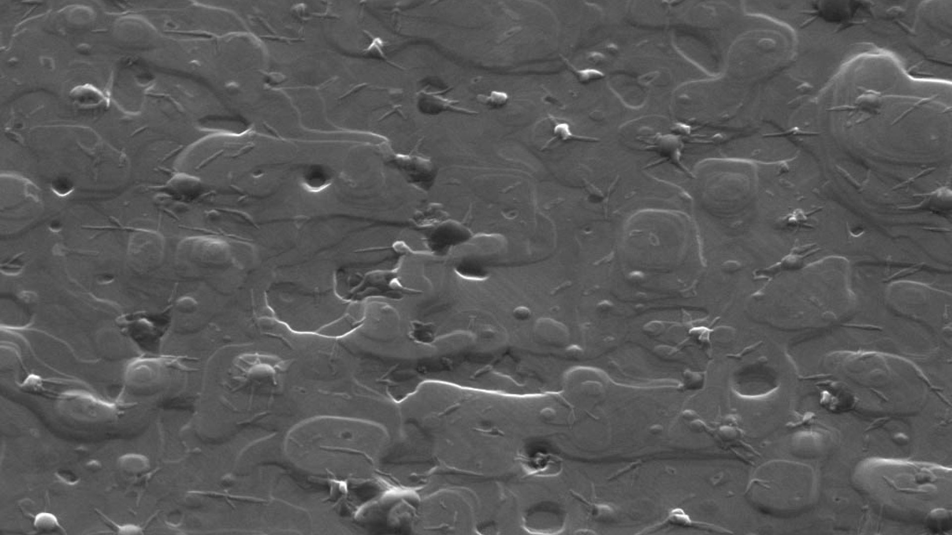
- SEM pictures of different materials obtained by the Scanning Electron Microscope QUANTA FEI 200 FEG-ESEM
Equipment TEM
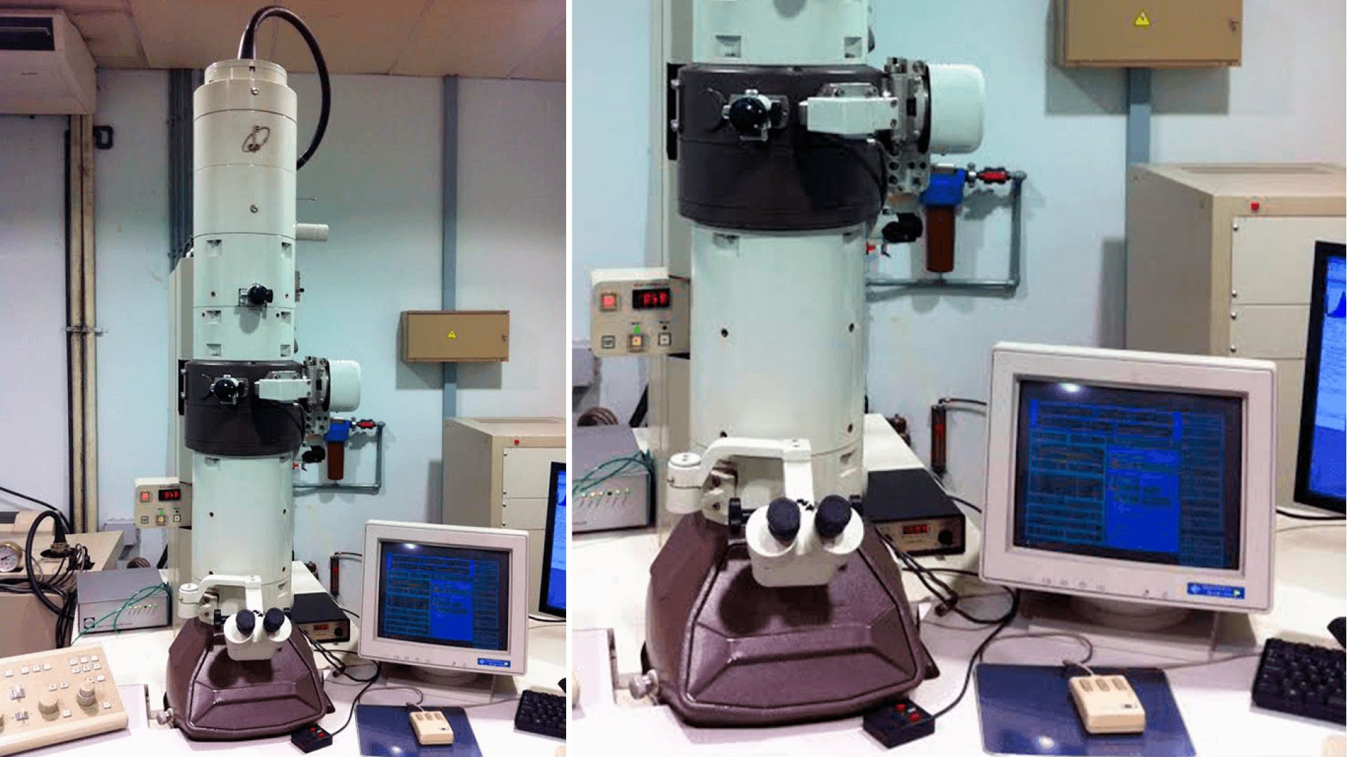
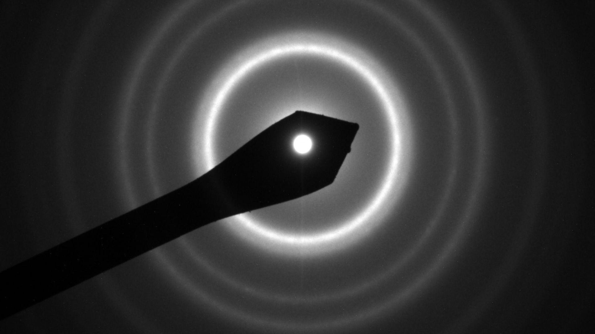
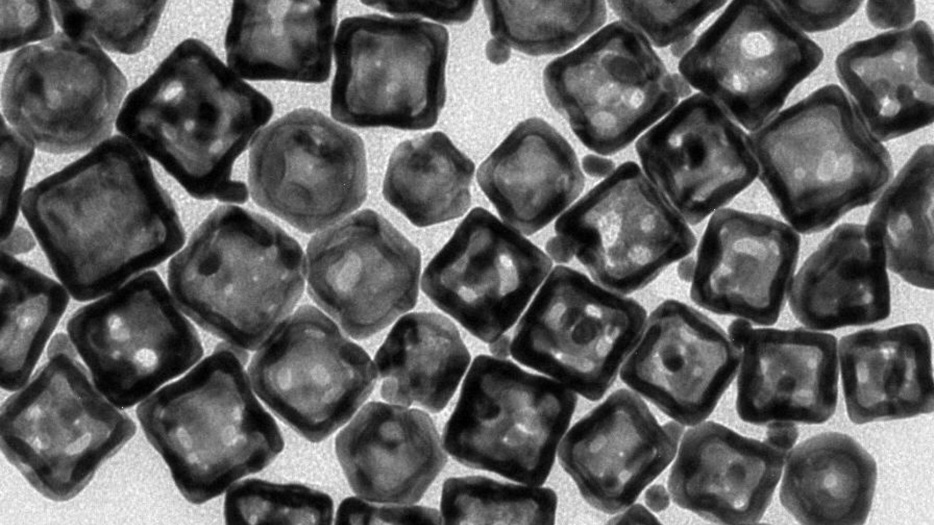
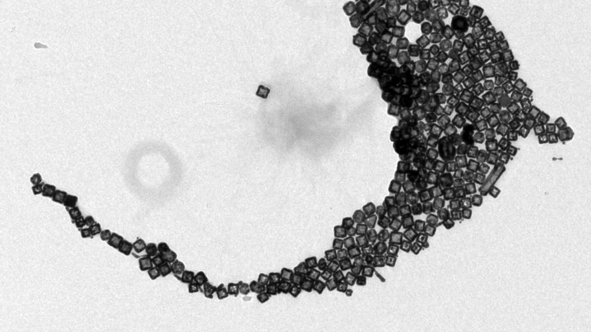
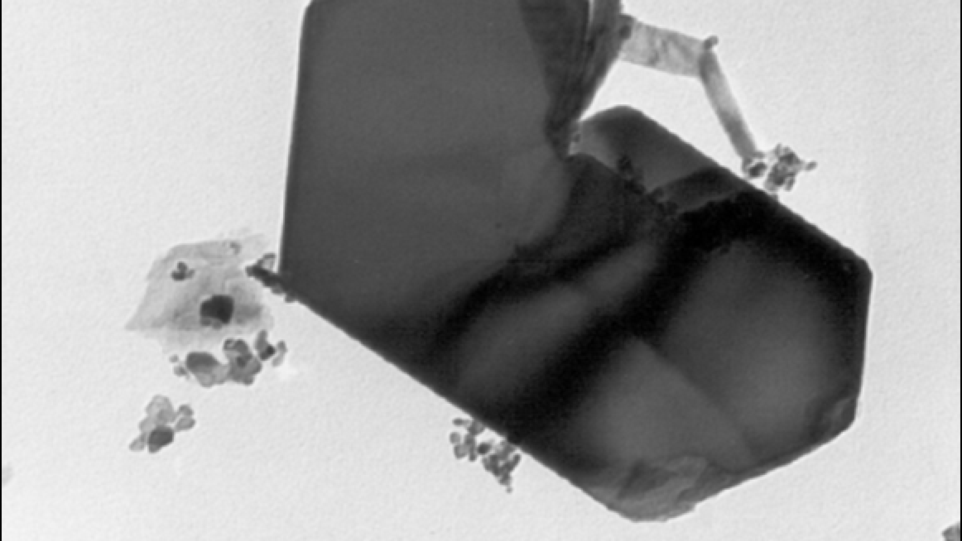
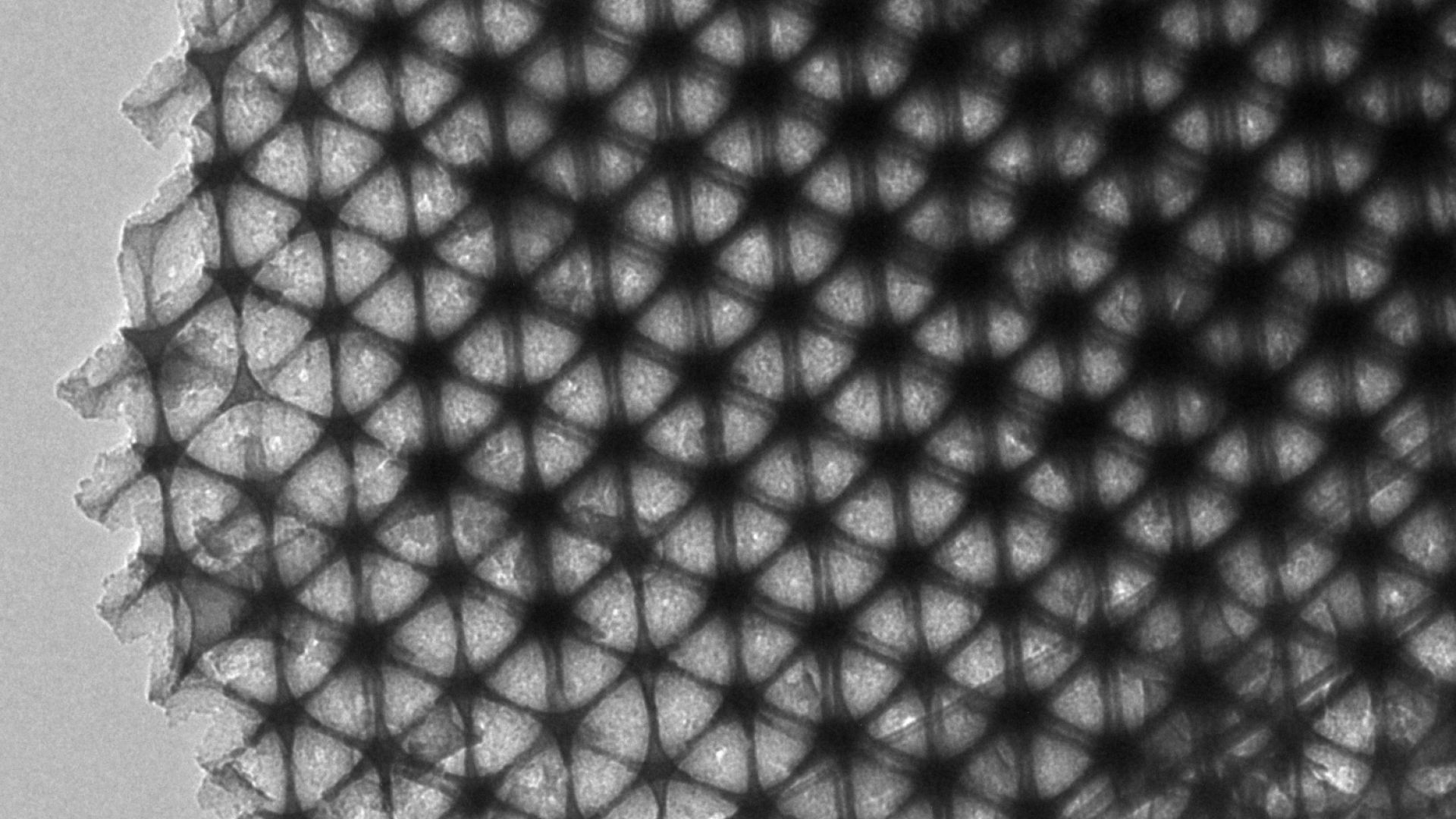
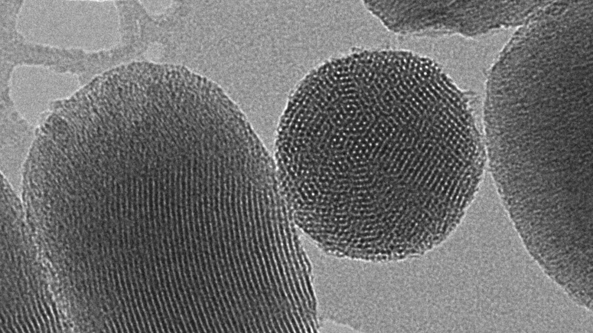
The 120 KV JEOL 1210 TEM features a high angular range (Tilt X= ± 60o, Tilt Y= ± 30o) providing a unique facility in the area of Barcelona for exploring large volumes of the reciprocal lattice by electron diffraction. It has technical support by a high profile (Dr) staff member. With a resolution below 3.2 Å this equipment is useful for low resolution structure imaging and characterization of nanoparticulate systems.
When operating in image mode TEM provides information about the size, morphology and microstructure of the samples.In diffraction mode, it allows the determination of the cell parameters, space group and superstructures, incommensurate modulations, etc. The transmission electron microscope service is equipped with:
- Holder: Analytical specimen holder, doble tilt ( Tilt X=± 60o, Tilt Y=± 30o ) GATAN 646.
- Camera: ORIUS 831 SC 600, GATAN.


Electron Microscopy
Service
Address:
ICMAB
Campus UAB
(in front of Firehouse)
08193, Bellaterra
Spain
E-mail:
-
This email address is being protected from spambots. You need JavaScript enabled to view it. -
This email address is being protected from spambots. You need JavaScript enabled to view it. -
This email address is being protected from spambots. You need JavaScript enabled to view it.