

P. O. Vaccaro, M. I. Alonso, M. Garriga, J. Gutiérrez, D. Peró, M. R. Wagner, J. S. Reparaz, C. M. Sotomayor Torres, X. Vidal, E. A. Carter, P. A. Lay, M. Yoshimoto, and A. R. Goñi. AIP Advances 8, 115131 (2018)
https://doi.org/10.1063/1.5050674
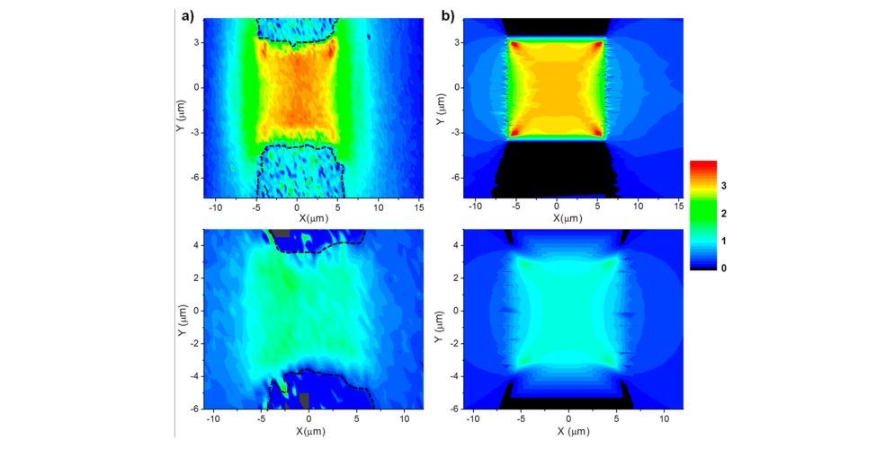
We deposited Ge layers on (001) Si substrates by molecular beam epitaxy and used them to fabricate suspended membranes with high uniaxial tensile strain. We demonstrate a CMOS-compatible fabrication strategy to increase strain concentration and to eliminate the Ge buffer layer near the Ge/Si hetero-interface deposited at low temperature. This is achieved by a two-steps patterning and selective etching process. First, a bridge and neck shape is patterned in the Ge membrane, then the neck is thinned from both top and bottom sides. Uniaxial tensile strain values higher than 3% were measured by Raman scattering in a Ge membrane of 76 nm thickness. For the challenging thickness measurement on micrometer-size membranes suspended far away from the substrate a characterization method based on pump-and-probe reflectivity measurements was applied, using an asynchronous optical sampling technique.
M4NRG Clean Energy
Localized thinning for strain concentration in suspended germanium membranes and optical method for precise thickness measurement

