


Perovskite nanocrystals (NCs) have revolutionized optoelectronic devices because of their versatile optical properties. However, controlling and extending these functionalities often requires a light management strategy involving additional processing steps.
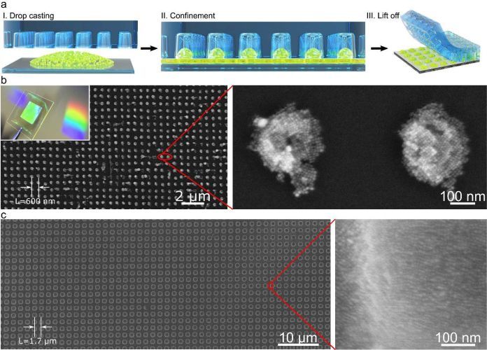
Here, we introduce a simple approach to shape perovskite nanocrystals (NC) into photonic architectures that provide light management by directly shaping the active material. Pre‐patterned polydimethylsiloxane (PDMS) templates are used for the template‐induced self‐assembly of 10 nm CsPbBr3 perovskite NC colloids into large area (1 cm2) 2D photonic crystals with tunable lattice spacing, ranging from 400 nm up to several microns.
The photonic crystal arrangement facilitates efficient light coupling to the nanocrystal layer, thereby increasing the electric field intensity within the perovskite film. As a result, CsPbBr3 2D photonic crystals show amplified spontaneous emission (ASE) under lower optical excitation fluences in the near‐IR, in contrast to equivalent flat NC films prepared using the same colloidal ink. This is attributed to the enhanced multi‐photon absorption caused by light trapping in the photonic crystal.
Templated‐assembly of CsPbBr3 perovskite nanocrystals into 2D photonic supercrystals with amplified spontaneous emission
Lakshminarayana Polavarapu, David Vila-Liarte, Maximilian W. Feil, Aurora Manzi, Juan Luis Garcia-Pomar, He Huang, Markus Döblinger, Luis M Liz-Marzán, Jochen Feldmann, Agustín Mihi.
Angew. Chem. Int. Ed.. Accepted Author Manuscript, 2020
DOI:10.1002/anie.202006152
M4NRG Clean Energy
Templated‐assembly of CsPbBr3 perovskite nanocrystals into 2D photonic supercrystals with amplified spontaneous emission

